New Ansys Tools Improve Semiconductor Design
Ansys Totem-SC and PathFinder-SC optimize power and reliability for automotive, 5G, and high-performance compute semiconductors.
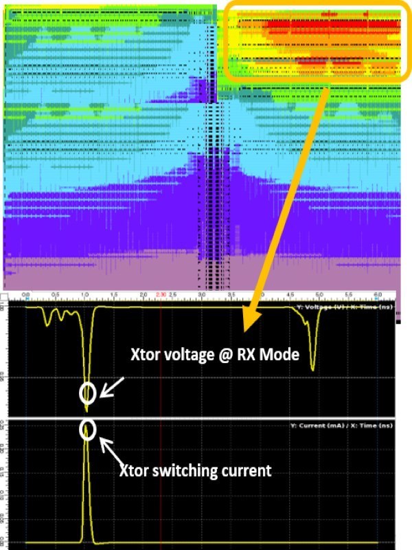
Ansys Totem-SC showing region of voltage drop in the power grid. Image courtesy of Ansys.


Latest News
June 23, 2022
Ansys has relesed two new semiconductor products – Ansys Totem-SC and Ansys PathFinder-SC – for power integrity and electrostatic discharge (ESD) reliability signoff, respectively. According to Ansys, the new products increase the speed and capacity of existing Totem and PathFinder products by integrating them into the Ansys SeaScape big-data platform for distributed processing. T
Totem-SC is built on the SeaScape platform to address the growing challenge of power integrity analysis in today's extremely large memory and analog mixed signal designs. SeaScape is a massively scalable data platform that used big-data techniques to enable highly scalable elastic compute and facilitate multiphysics analyses. According to the company, Totem-SC delivers 10x faster performance on average for dynamic voltage drop signoff of next generation designs like complementary metal oxide semiconductor (CMOS) image sensors, dynamic random-access memories (DRAM), flash memories, field programmable gate arrays (FPGAs), and high-speed transceivers.
“Power supply noise is a critical metric for our CMOS image sensors as it directly impacts pixel performance,” said Seonil Brian Choi, Corporate VP Samsung Electronics. “Totem-SC offers us a high-capacity IR signoff solution for Samsung's high-resolution sensor designs using standard low-memory machines. The high-fidelity results give our team the confidence to maximize design optimization for a better final product.”
PathFinder-SC provides a high-capacity solution for verifying the protective circuitry found on all chips that protect them from electrostatic discharge (ESD) and damage from voltage spikes. This technology has increased in importance as silicon technology continues to shrink to 7nm and below where tiny transistors need to be protected by critical ESD circuitry that is checked, verified, and signed off with PathFinder-SC. SeaScape technology allows PathFinder-SC to deliver 10x faster turnaround for ultra-large SoCs, the company says, which makes it applicable for large, high-speed semiconductor designs in artificial intelligence, imaging, networking, and 5G and 6G telecommunications.
“ESD signoff has become increasingly challenging as our design has grown larger and the predictive accuracy requirements have tightened,” said Chanhee Jeon, Master (VP of Technology) at Samsung Electronics. “We have found that PathFinder-SC gives us a high-capacity ESD signoff solution with superior root-cause analysis and multiphysics analysis capabilities, which helps us meet our delivery schedules.”
The SeaScape platform is an open platform architecture that allows customers to integrate other tools and their own algorithms by means of a Python-based customizable user interface (UI).
“Designing today's chips and electronic systems is an increasingly complex multiphysics analysis and simulation problem that requires a broad array of tools to solve,” said John Lee, vice president and general manager of the electronics, semiconductor, and optics business unit at Ansys. “Ansys strongly believes in providing open and extensible platforms like SeaScape so our users can use the best tools to simulate, analyze, and optimize their product designs – all the way from early prototyping to manufacturing signoff.”
Sources: Press materials received from the company and additional information gleaned from the company’s website.
More Ansys Coverage
Subscribe to our FREE magazine, FREE email newsletters or both!
Latest News
About the Author
DE’s editors contribute news and new product announcements to Digital Engineering.
Press releases may be sent to them via DE-Editors@digitaleng.news.