
Latest News
October 14, 2022
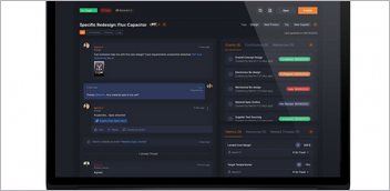
Cadence Design Systems, Inc. establishes a collaboration with Google Cloud that is said to accelerate system and semiconductor design with cloud-ready tools included in the Cadence Cloud Passport that have been certified for use with Google Cloud. This collaboration is made to provide engineers with improvement in design and verification throughput. Cadence tools have been tested and benchmarked on Google Cloud.
Google silicon teams have used Cadence cloud-ready tools for verification, implementation and system analysis workloads on Google Cloud, leveraging flexible consumption models by Cadence. The Google silicon teams successfully developed the Tensor system-on-chip (SoC) and Tensor Processing Units (TPUs) using Cadence cloud-ready tools running on the Google Cloud GCP high-performance computing-optimized infrastructure. Google silicon teams also used the Cadence Jasper Formal Verification platform in the cloud to improve the reliability of TPU designs.
“We’re excited to collaborate with Cadence to bring their modeling and simulation software to Google Cloud customers,” says Sachin Gupta, VP and GM of Infrastructure, Google Cloud. “Together we bring unprecedented functionality, scale, and access, which will enable the next wave of innovative industry products in the electronic design and computer-aided engineering market segments.”
“By furthering our collaboration with Google Cloud, we’re helping customers leverage the massive scalability of the cloud and improve overall design productivity,” said Nimish Modi, senior vice president and general manager, Strategy and New Ventures at Cadence. “Combining the power of our computational software with Google Cloud high-performance compute gives our customers access to a proven solution that provides a competitive advantage.”
The Cadence Cloud Passport is part of the broader Cadence Cloud Portfolio, which offers customers flexible access to Cadence tools in the cloud. The Cadence Cloud Passport and Cadence Cloud Portfolio align with the company’s Intelligent System Design strategy, enabling SoC design. More information can be found here.
Sources: Press materials received from the company and additional information gleaned from the company’s website.
More Cadence Coverage
Subscribe to our FREE magazine, FREE email newsletters or both!
Latest News
About the Author
DE’s editors contribute news and new product announcements to Digital Engineering.
Press releases may be sent to them via DE-Editors@digitaleng.news.