Additive Manufacturing Solutions for Silicon Wafer Tooling
Industrial additive manufacturing solutions can optimize the hardware and tools in microchip fabrication production lines.
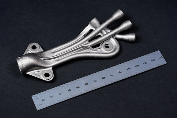
Figure 1. Additively manufactured cryogenic manifold produced on 3D Systems’ DMP 350 platform.
Latest News
March 23, 2021
Microchip fabrication is considered state-of-the-art in advanced manufacturing. This is an industry driven by the pursuit of faster, more efficient processors and higher capacity memory chips where we see racing vectors driving ultra-high levels of detail fidelity, resolution, and precision, all wrapped within massive investments in advanced tooling systems and infrastructure. Multi-billion-dollar production lines depreciated over billion-unit production runs present staggering metrics, as well as massive continuous optimization initiatives. When it comes to optimizing the hardware and tools that exist within these production lines, the emergence of industrial additive manufacturing (AM) solutions has started to present a significant opportunity to engineers and designers at the very front line of problem-solving.
Phenomena
Within silicon wafer tooling there are many complex phenomena with which to interact. Temperature, inertia, turbulence, resonance, vibrations, precision, wear-and-tear as well as ultra-high levels of pristine clean driven by zero tolerance for contamination, converge to present a significant challenge, while at the same time many opportunities for optimization. This is where AM comes in.
Additive manufacturing allows for step changes in component performance and efficiency. With the traditional rules of design and manufacture that you see in conventional parts, performance is always somewhat compromised. With AM, specifically by embracing design for additive manufacturing (DfAM), the philosophy of ‘design for function’, enables companies at the front line of problem-solving to innovate in ways previously never considered possible. Historically, ‘design for manufacture’ was constrained by the relationship between cost and design sophistication. AM breaks this equation. Take for example cryogenic tubes and manifolds.
Fluid Flow
Traditionally these very complex circuity components are time-consuming and difficult to fabricate, requiring multiple manufacturing processes from sheet metal folding to hydroforming and tube bending, all integrated with assembly steps. The net result never quite approaches the perfect solution, due to assembly processes and steps that are full of potential points of failure. The braze lines themselves present surface imperfections that can impact the smooth laminar flow. When AM is applied, designers can present the perfect tubular system utilizing advanced fluid flow CFD to influence, and in some instances automate, the creation of form as well as the integration of sophisticated baffle strategies, that allow for minimizing turbulence while maximizing flow efficiency. The benefit of such architectures is the minimization of vibrations and resonance that correlates with net turbulence within systems as depicted in Figure 1.
Turbulence and vibrations impact the precision of output, and in a world where nanometers count, this presents significant capability. Finer fluid flow within these plumbing systems equates to higher precision and better yield. Using 3D systems’ Direct Metal Printing (DMP) 350 platform engineers were able to realize a 90% reduction in liquid-induced disturbance forces to reduce system vibration and realize 1-2 nm accuracy improvement.
Part Count Reduction
An added benefit of AM is being able to grant the designers access to significant levels of component consolidation, which ultimately drives the design efficiency principle of ‘part count reduction’ leading to the expression of complex manifolds as monolithic components with no assembly required. This simplifies not only supply chain lead time but even makes the process of design easier. This time saving can be significant. In some examples, we have seen months become hours - driven by the removing the need for tooling, assembly, and the associated inspection process. We have seen up 50x reduction in part counts under component consolidation within some of these complex systems.
Thermal
Another example where we see AM presenting step changes in capability is wafer tables as shown in Figure 2 that are used for handling and fixturing the silicon plates during the manufacturing process. Similar to cryogenic tubes and manifolds these components need to transmit and distribute super cooled cryogenic fluids. However, in this case, the primary challenge is managing ultra-fine levels of thermal consistency. Thermal variation causes minute changes in the expansion of materials. Thermal gradients and fluctuations over time can create scenarios where the position of structural elements being printed and accumulated on the surfaces of the silicon wafers can shift. The bottom line is thermal variation can impact the precision of process as well as resolution of tool capability. To solve this, engineers are turning to AM to design, develop and manufacture next-generation silicon wafer table architectures. Again, unconstrained by the limitations of traditional manufacturing and assembly methods these plates can access unparalleled levels of performance.
![]()
Figure 2: Silicon wafer table with integrated advanced cooling structures (cut-away section) produced using 3D Systems’ DMP 350 platform.
For example, by utilizing 3D Systems’ additive manufacturing solutions, one silicon wafer tooling company was able to realize a 6x improvement in thermal performance and a 5x stabilization improvement. The thermal profile within the conditioning ring was able to see a ΔT improvement from 13.8 to 2.3 mK, with a thermal temperature gradient reduced from 22 to 3.7 mK, in a more responsive system presenting a time constant moving from 7s to 1.5s. In fact, the efficiency, performance, and responsiveness of the AM architecture were so high that the engineers were able to look at actually regressing an alloy selection from expensive copper to cheaper and lighter aluminum—an unanticipated benefit of a DfAM design optimization functionality offset.
Mass
Down selection of alloys to cheaper lower density materials is just one driver of weight reduction. DfAM generally presents significant opportunities for more efficient design through bulk material savings. When you don’t have to design for assembly and break out from under the constraints of traditional manufacturing processes, ‘lighter weight’ has multiple benefits. These include lower thermal mass which, as mentioned above, results in faster thermal condition response. Lower inertia results in opportunities for faster and higher precision conveyance, more precise stop and start acceleration/deceleration profiles, while at the same time reducing wear and tear of mechanisms. Less wear and tear results in less downtime, less maintenance, as well as improved capacity. Reduced mass/inertia combined with DfAM-based improvements in the stiffness of subcomponents in high-velocity reciprocating mechanisms also reduces the generation of vibrations within systems. Again, like in the high flow rate manifolds, reduced vibration improves the overall precision and resolution of the system—a high-value lever in the pursuit of higher resolution higher density processors. At a silicon wafer tooling company, engineers were able to realize 50% weight reduction for reduced inertia, with a boost in stiffness of 23% resulting in a higher resonant frequency and reduced system vibration, all equaling improved speed and productivity.
Flexures
Another very interesting and somewhat novel field to emerge as a function of advanced DfAM in silicon wafer tooling is the integration of mechanisms. Whereas all examples presented so far have covered static and monolithic sub-components and parts, integrated mechanisms combine some of the principles of kinematics and flexures to enable dynamics. The 3D Systems DMP 350 platform has a unique capability in this space.
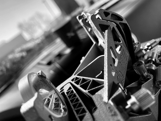
Figure 3: Integration of flexures into monolithic mechanisms (Part courtesy of VDL).
One, in particular, is related to the build environment within the DMP system itself. Ultra-low O2 levels of <25ppm allow for the expression and processing of ductile cyclic fatigue-resistant titanium. With ductility, engineers are now able to explore functional leaf springs and flexures. With access to flexures VDL, for example, was able to successfully manufacture advanced optical assemblies with monolithic integrated mechanisms as shown in Figure 3. Flexures presenting full fine control adjustability with all the benefits of massive levels of part count reduction, and lead time compression ultimately allowed engineers to design and produce faster, cheaper, and higher precision optical assemblies and other advanced mechanisms.
The rate of optimization in silicon wafer is not slowing down. If anything, it’s accelerating. And as we’ve seen AM is playing—and will continue to play—a significant role in enabling the slope of the curve. Additive manufacturing is here to stay. We’re at the beginning yet barely scratching the surface, but the value has already proven to be significant. As more and more silicon wafer tooling engineers at the front line of problem-solving become aware of the capability of additive manufacturing (and combine it with their creativity) they will take these advanced workflows to a whole new level.
Patrick Dunne is Vice President, Application Development, at 3D Systems.

More 3D Systems Coverage
Subscribe to our FREE magazine, FREE email newsletters or both!
Latest News